Industrial Design

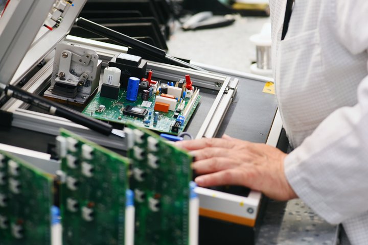
Design can make a big difference in exceptional PCB assembly: in functionality, but also in efficiency, and therefore in cost price. We therefore pay the utmost attention to it. We recognize two phases: design for manufacturing and design for testing. But we also add a mentality: design for cost.

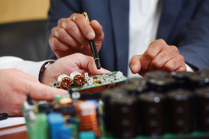
Design for manufacturing

In this phase, we examine whether we can produce your PCBs at an industrial scale. Also we look for the smartest way to do this. We definitely don’t try to do the engineer’s work for him/her, but we do think about how to optimize the process.

A different component, a different layout, adjustments to the form: these can make the difference between ‘producible’ and ‘efficiently producible’.

PCB product engineering

Design for testing

With the test platform NedFlex® which we designed ourselves, we subject every product to a series of exhaustive (inline) tests prior to production. These tests identify any defects at an early stage, and provide valuable data. The data then help us to realize a high degree of coverage, and therefore reduce your costs.

All test disciplines

  • ICT In circuit testing
  • FPT Functional product testing
  • AOI Automatic Optical Inspection
  • BI/RI Burn-in/Run-in (reliable)
  • X-ray inspection
  • HV High voltage (isolation) testing
  • RF Radio frequency testing
  • EOL End of line testing (mechanics/housing)
  • LT Leakage testing

Custom PCB fixture development

Design for cost

Design for cost is not a tool or a method, but rather a mentality.
In each phase of the design and production process, we study how things can be made faster or more efficient. After all, we both benefit from that.

State-of-the-art production plant

Exceptional PCB assembly demands a high-quality production location. Explore our energy neutral plant in Slovakia.

Explore our production plant
Let us help you to
take the lead

Download company presentation

Feel free to get to know our company even better.

Download now

Semecs Company Presentation