PCB manufacturing
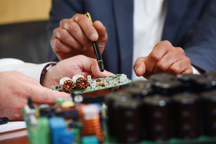
At Semecs, we are fully geared towards serial production. We usually produce orders in volumes of 5.000 pieces to 500.000+ pieces. Our greatest strength in industrial-scaled assembly is our flexibility.
With our flexible lines and processes, we can adapt immediately to the inevitable changes in the market.
And whether it is the start of the electronics manufacturing services process or the end of the product life cycle: you can count on us. That is what we call exceptional PCB assembly. Certain parts of the PCB fabrication process require extreme precision. That is why we are making substantial investments in robotization.

Our PCB manufacturing competences
- Traceability
- Surface-mount technology
- Depaneling
- Through-hole technology
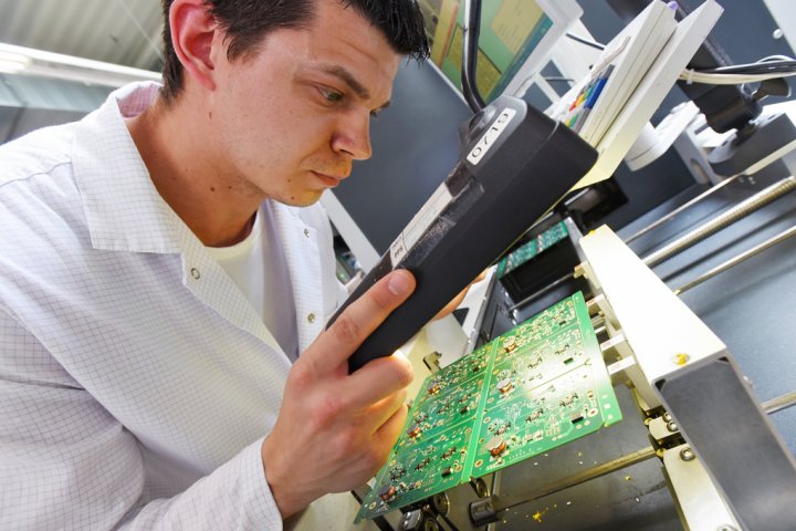
- X-ray analyzing & Examining
- In-circuit and functional testing
- Conformal coating
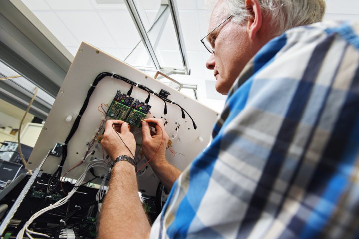
- Box building

PCB fabrication
The Semecs team offers PCB fabrication in volume between 5,000 and 500,000 pieces. Even though PCB fabrication doesn't include the PCB design, our team offers flexible design solutions to enhance the final product quality and optimize the fabrication time. PCB fabrication presents the procedure to convert feed materials from a circuit board design to a physical structure based on the design package's specifications. Before the manufacturer can build the raw board, a checklist of design details must be complete. Once the design specifications between the client and manufacturer are agreed upon, the PCB fabrication can take place. The PCB fabrication is the first part of the PCB manufacturing process. All board layers are prepared and bound together. The inner layers structure and electrical circuits are formed under UV light where excess copper is etched away. Then holes are drilled into the board, and the board is coated with a thin film that protects it from corrosion. After that, the board is ready for the second part of PCB fabrication which is PCB assembly, where all components are mounted, and the board is ready for application.
PCB production
Here at Semecs, the first stage of PCB production is a review of the design provided by our customers. Our team of engineers internally reviews the design and checks whether it contains sufficient information to start with the PCB manufacturing. If that is not the case, our team either suggest possible design additions or requires missing specification from the client according to his specific needs. Then our team prepares all necessary production tools and starts ordering electrical elements and feed materials in demand from our established suppliers.
The PCB production starts with the preparation of raw materials such as chosen substrate material and copper sheets. Then, they have to be shaped appropriately to minimize waste generation during the production process. Once materials are prepared, the special printers make a photo film on the material's surface. The film is an actual depiction of PCB. Hence its application onto the layer's surface must be highly precise. The photo film resistance to UV rays is an essential trait that enables the removal of the excess parts and forms the inner layers the same way they are digitally designed. The aim of efficient PCB production is high product throughput, so our customers can get their products promptly. We at Semecs can deliver high PCB quantities in a short period due to the usage of the latest manufacturing PCB technology.
PCB technology
Many manufacturers specialize in only one PCB technology, but that is not the case with the Semecs. We at our facilities gained expertise in both surface mount technology and through-hole technology. Even if it requires more time and more manual work, the through-hole technology is still necessary for some applications. This technology is the client's first choice when PCB is placed in a harsh environment and subjected to mechanical stress. So, our specially trained staff proceeds with this technology that also includes machines and special process design.
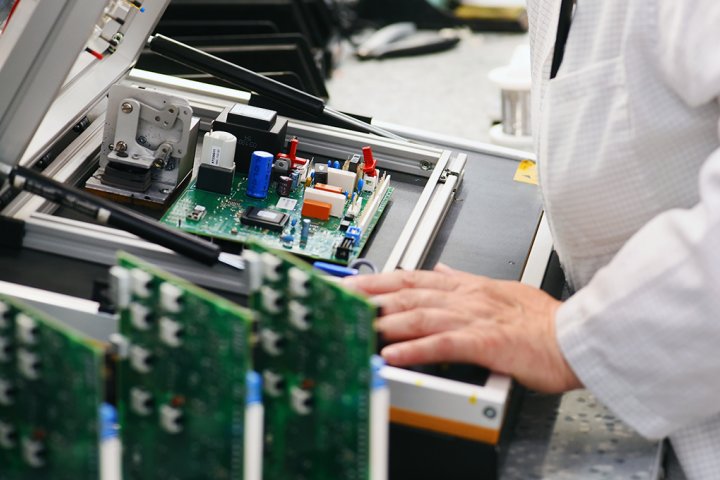
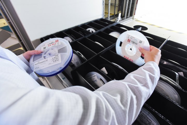
On the other side, we offer PCB assembly using state-of-art surface mount technology. We offer a fully automated production process using this type of PCB technology. Our machines are easily integrated with data from the Gerber file that present the input parameters. The pick and place machine is used for component placement while our staff supplies the machine with all needed SMD components for particular PCB manufacturing. The PCB technology consists of three steps: solder paste printing, components placement, and reflow soldering. In the end, our technicians visually check the boards, and if they do not detect any defects, the boards are ready for functional testing. Once the testing is passed, the PCB is ready for shipment.
Print circuit board structure and purpose
A printed circuit board is a core of an electronic system. It enables electricity, signal, and data transfer from sources to targets. The print circuit board has two primary functions: allowing the stable attachment of electronic components on one side and allowing electrical interconnection between them on the other. The electricity flow between electronic components within the PCB is enabled via conductive paths, tracks, or signal traces etched from copper sheets lanated onto a non-conductive substrate. The PCB must maintain high performance during its lifespan to prevent transfer delays or inaccurate data transfer.
PCB substrate materials
Some of the widely used substrate materials in PCB manufacturing are epoxy, polyamides, polyethylene terephthalate, and polyethylene naphthalates due to their physical and chemical properties. Still, the most used substrate in PCB manufacturing is a glass fiber reinforced (fiberglass) epoxy resin with a copper foil bonded to one or both sides. Due to its firm structure and durability, fiberglass provides exceptional mechanical strength. The fiberglass layer is covered with an epoxy resin that is an excellent electrical insulator and flame-resistant material, which is essential since some electrical components' temperature rise is common.
PCB sides
In terms of their functions, the PCB has two sides, where the top side is used for component attainment in the case of a through-hole board, while the bottom side is widely known as the solder side since it touches solder wave during assembly. The PCB is often assembled of multiple thin layers whose sum thickness must be within a specific size range specified by a customer. Since design standards and constraints are getting stricter from year to year, PCB manufacturers must always follow the latest technology trends in various fields, especially in medical, automotive, and industry.
What is PCB manufacturing, and how is it done
Digital and actual PCB design
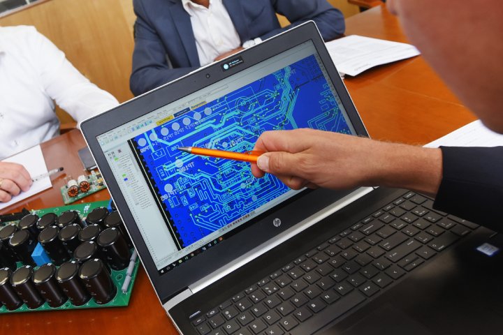
Every custom PCB design is a result of the specific needs of customers in the electronic industry. The designers proceed with the PCB design according to their requirements using specialized software. The final results of their design is a blueprint of the custom PCB, which must contain all needed PCB specifications so manufacturers can proceed with PCB manufacturing.
Before PCB design, designers should consult with manufacturers about the compatible software to avoid any potential issues during the manufacturing phase. The problems can arise from discrepancies resulting from the designer's software calling wrong sequences in Gerber file generation. Even though particular software encodes all technical specifications about the PCB, such as copper tracking layers, drill drawing, apertures, and component notations, the transferred data into manufacturer software may not be the same as the original one. Therefore, particular attention is needed during PCB design to avoid repeating the design process multiple times.
Once the designer completes the PCB design, he runs its check performed by software that uses oversight algorithms to ensure no short circuits or other errors are present. Designers also deliver the following specifications: track width, board edge spacing, trace and hole spacing, and hole size. After a successful feasibility check, designers forward the PCB file to the PCB manufacturing company.
To ensure the design fulfills requirements for the minimum tolerances during the manufacturing process, almost all manufacturing companies perform a Design for Manufacture (DFM) check before circuit board manufacturing. To successfully proceed with PCB manufacturing, curing and shaping the substrate is essential. Firstly, the substrate is cut according to the required size of the PCB. After achieving the final shape, the material must pass through the oven, where it's exposed to a 150 degrees Celsius temperature for 3 to 4 hours. The substrate curing ensures the material's additional hardening. At the same time, highly toxic volatile organic compounds are released in the oven, ensuring that there is no release of toxic substances from PCB after being manufactured.
When a substrate is ready, the transformation of the digital PCB into an actual one may begin with the PCB printing process. PCB manufacturers use so-called plotters that belong to the laser printers group for printing purposes, but their design and operating mechanism are different from the standard laser jet printer. The main difference is that plotter utilizes more precise printing technology to provide a clear and visible depiction of all details presented in the produced film. The film comprises two layers types, inside and outside ones. The inside layers contain two ink colors where black ink represents copper traces and electrical circuits while clear ink represents non-conductive areas. In contrary to the inner layers' design, the outer layer design is reversed. Clear ink represents copper pathways, while black ink represents areas where the copper will be etched away. Every single PCB layer and corresponding solder mask have their unique film. After films of all designed layers are printed, they are aligned with the highest precision, and then the registration hole is pierced through all films. The accuracy of the hole position is achieved by adjusting the table position on which the film sits. The holes will fit into the registration pins in the imaging process.
Creation of electric circuits within inner layers
The primary goal of the film fabrication is to make an exact map of the copper pathways-electric circuits. Electric circuits within inner layers are created by printing the copper pathways from the film onto copper foils. To enable PCB longevity and fulfill our customers' expectations, Semecs use a sterilization process to remove the most tin parts that could cause short or open circuits. Once the film is attained onto a copper foil, the clean panel receives a highly reactive photo-sensitive chemical layer, often called photo resist. The photo-sensitive chemical forms a tiny film that hardens when exposed to a UV light of a particular wavelength. The hardening process ensures that the exact pattern from the photo film is transferred to the photo resist. The films fit onto pins that hold them in place over the laminate panel.
Since only white parts of the inner layers’ printed film should remain within the PCB, the UV light passes through those parts while simultaneously hardening the photo resist on the copper underneath. Since black color from the printed film completely absorbs light, it prevents hardening the areas that shouldn't harden. When the PCB inner structure is formed, the board is washed by an alkaline solution that cleans photo-sensitive chemical residues that didn't harden. Often the additional application of deionized ultra-pure pressurized water ensures complete removal of all undesired particles. After cleaning, the board undergoes a drying process, so moisture that could cause short circuits is wholly removed. After the drying process, the inner layer copper structure is completed, while surface cooper excess is left for removal later on.
Permanent interconnection of layers
Once all layers are finalized, they must be aligned with the micro-precision. The layers are aligned using either mechanical drill or laser where laser hole diameter is regularly below 0.2mm while mechanical drill hole has diameter 0.3mm or less. Before punching holes, the technician place all layers in the machine called the optical punch, which allows an exact alignment of all layers enabling accurate punching of registration holes. Quality assurance is performed by another machine that does optical inspection. During this phase, the device provides information about the absence or existence of defects and misalignment. Also, the device compares the original design from Gerber, which the manufacturer received, with aligned layers. The machine scans the layers using a laser sensor and electronically compares the digital image with the original Gerber file.
Due to pierced holes, aligned layers are firmly connected, while outer layers shall bond with the substrate. This process compromises 2 consequent steps: layer-up and bonding. In the layer-up part, metal clamps fix all layers on a special press table. Then layers are mounted onto pins attached to the table to prevent the misalignment under pressure during the fusion process.
The layer up process goes in the following sequence:
- Firstly the substrate layer fits over the epoxy resin, widely called prepreg.
- Secondly, the copper sheet fits on the substrate layer.
- Thirdly, further sheets of prepreg are placed on the top of the copper layer.
- Lastly, one more copper layer is placed on the top of all assembled layers, which acts as the press plate in the following process.
Once the layer-up process is finished, the technician takes over the layer stack to a laminating press. This press applies both pressure and heat by using a pair of heated plates. The generated heat melts epoxy, which then forms firm chemical bonds with the neighbor layer. After the pressing process, the technician removes the top press plate as well as previously attached pins.