Surface-mount technology is our favorite technique that we use here at Semecs production facilities. This technique is famous for its high efficiency and the wide range of flexible solutions it offers. It wouldn't even come into existence if the rise of surface-mounted devices (SMDs) didn't occur as well as the invention of their assembly. The SMD's specific design showed dominance upon traditionally used through-hole electronic packages that required large PCB space and manual mounting of lead into holes. The SMDs passed through many development phases until they fulfilled all electrical and mechanical properties requirements for successful SMD assembly.
Besides SMDs structure, the two other factors were critical for successful SMD assembly. Firstly, the discovery of materials suitable for connecting with pins that don't affect electric conductance and cause open circuits. Besides containing metal powder that melts during the soldering phase, the solder paste must own adhesive property to hold components firmly before and during the soldering stage. Secondly, once appropriate materials were developed in the form of the solder paste, there was a need to design a process that will permanently fix SMDs to printed circuit boards. The soldering under high temperatures where paste transforms in the solid became the standard technique for permanent mounting electronic components onto boards. The innovation in terms of soldering under high temperatures challenged a material scientist to discover optimal materials that will be great insulators to electric components by having high thermal resistance values.
SMD components classification
Surface-mounted devices (SMDs) are electronic components attached to printed circuit boards during the SMD assembly process. Regardless of size and shape differences, the SMD components are regularly classified based on their electronic functions.

Passive SMD components - Capacitors and Resistors
Passive SMDs are electrical components that are used to adjust the voltage and amperage of the electric current. Naturally, the capacitors and resistors are the main components of this group. Other components that present a minor part are crystals and coils, and due to specific requirements, they are often custom-made. Therefore, there are no widely used standards regarding their manufacturing. On the other side, the resistors and capacitors are manufactured in a standardized manner. These components may possess the following standard labels: 1812, 1206, 0805, 0603, 0402, and 0201. The figures refer to the dimensions in hundreds of an inch. Therefore, the 0201 measures 2 x 1 hundredths of an inch. The PCB size requirements are getting smaller while the density of the components positioning in the single board increases. Nowadays, the larger sizes are rarely used due to their robust structure and their occupation of large board spaces.
Resistors are divided into two distinct groups based on their assembly. Chip resistors are made of various materials to reach designed resistance. In contrast, network resistors are built of multiple resistors of the same resistance connected in series to divide the voltage properly. Both resistor types are labeled with three digits. The three digits are printed on the resistor body to indicate the resistance value. The first and second digits represent significant digits, while the third digit is the power of 10 that multiples the first two digits. Therefore 352, is a label for 3500Ω.
Capacitors' primary roles are storing and releasing electric energy corresponding to their capacitance. There are multiple types of capacitors such as Electrolytic, Mica, Paper, Film, Non-Polarized, and Ceramic. Still, the most widely used capacitor in the SMD assembly is a multilayer ceramic capacitor (MLCC). It is a dielectric capacitor made from specific ceramic materials with excellent frequency response, high accuracy, and high thermal resistance that enables its long lifespan. Another desirable characteristic of ceramic multilayer capacitors is their small capacitance regularly in the range from 1F to 1µF, which is suitable for PCB manufacturing. The MLCC is divided into X7R, Y5V, and C0G (NP0).
C0G (NP0) is a class I ceramic material composed of neodymium, samarium, and other ferroelectric oxides. Its capacitance is incredibly stable with a maximum absolute error of 0.3% in the range from -55°C to +125°C. Furthermore, its specific capacitance change over a lifetime is less than 0.1%, which is over five times lesser than one of the majority of other capacitor types. Therefore, high accuracy over the participated lifespan, usually up to 20 years, makes this capacitor ideal for PCB assembly.
Diodes and transistors
Both diodes and transistors are semiconductors contained in the plastic package. They are connected to the printed circuit board via small leads mounted on the package. The leads are in direct touch with the solder paste positioned at particular places over printed circuit boards enabling the firm and stable bond. The purpose of the transistor is to amplify or switch electronic signals. That function is enabled with the help of three terminals: collector, emitter, and base connected to the circuit board. The emitter junction is forward bias and possesses a small resistance, while the collector junction is in reverse bias and possesses high resistance. On the other side, the diode is a two-terminal device that allows the current to flow only in one direction. Therefore, the electricity flow within the circuit occurs only when the diode is forward bias. The forward bias means the P-type material is connected to the battery's positive terminal, while the N-type material is connected to the battery's negative terminal. Therefore, the appropriate diodes' orientation during the pick and place phase is essential to achieve the proper SMD assembly.
Integrated circuits (IC)
Almost all printed circuit boards contain at least one integrated circuit. Their inclusion within the SMD assembly process is practically mandatory due to numerous roles they can perform, such as an amplifier, microprocessor, oscillator, and timer. Their outstanding advantages are their nominal size which is compatible with PCB design, and the ability to perform quite complex tasks simultaneously. They are manufactured in the form of chips using special equipment where dozens of transistors, capacitors, and resistors are packed inside the silicone shell.
Since they can perform complex tasks such as calculations and data storage using digital or analog technology, the microprocessors are the heart of the printed circuit boards. Digital technology can be found in PCs, networking equipment, and most consumer electronics, while analog technology is used in radio and audio frequency amplification. The main difference between those two is the way they perceive and process the received electronic signals. The Digital ICs use logic gates whose outputs are values of ones and zeros. There is a threshold in terms of the received signal's amplitude below which output is zero, while stronger signals result in the value of one. The threshold is programmed and specified for each gate in the integrated circuit by the engineer. On the other side, analog ICs receive signals that they continuously convert into programmed outputs using linear functions. The integrated circuits are also classified based on the number of transistors within the chip.
The categories are the following:
- Small (SSI) with less than 100 transistors
- Medium (MSI)- 100 to 10,000 transistors
- Large (LSI) - 10,000 to 100,000 transistors
- Very large (VLSI)- 100,000 to 1,000,000 transistors
- Ultra large (ULSI) with over 1 million transistors
Presented groups of integrated circuits also differ significantly in the number of required pins for connection with the board. For example, the small logic gates usually require between 14 to 16 pins, while the most widely used VLSI requires up to 200 and even more pins.
SMD assembly using surface mount technology versus through-hole mounting
Through-hole mounting is considered a traditional way of electronic components’ mounting, and it has numerous drawbacks. The holes are pierced in the deeper layers of the printed circuit boards to enable electric circuit connection with mounted components. Hence, all electronic components must possess wires with a diameter that perfectly fit the hole. The issue that arose with through-hole assembly is the insufficient strength of the bond that holds the wire in the hole. Further problems arose due to the necessity for manual placement of each electronic component to the board when required production throughputs reached hundreds of thousands of PCBs. As a result, this technique couldn't follow the modern hyperproduction requirements, so there was a need for its permanent replacement.
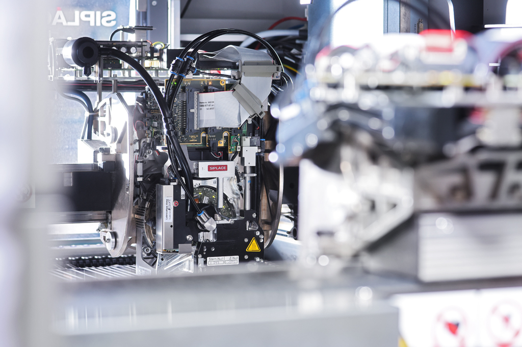
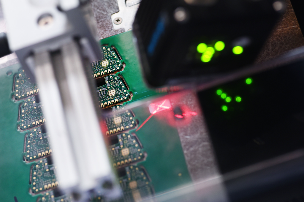
The Semecs team exclusively utilize the SMD assembly using completely automated surface mount technology that showed absolute dominance over the traditional through-hole assembly. Contrary to conventional assembly, surface mount technology utilizes pins attached to printed circuit boards by soldering them onto the pads. As a result, almost all SMD components are automatically mounted using a pick and place machine, with some minor groups that may require manual handling. The Semecs team often suggests alternate flexible solutions during the design stage so that all components can be mounted automatically. In that way, the mounting precision is significantly higher while production costs are reduced for the mutual benefit of both manufacturer and the client.
The rise of surface mount technology drove the need for excellent thermal resistance to protect electronic components from high temperatures during the soldering phase. The result of that need, in the last decades, is the invention of numerous insulating polymer packages that act as a shell of SMDs that contain electronic components within their structure. Furthermore, the capacitor's suitable structure was often questioned since widely used tantalum capacitors are flammable under higher temperatures. Even great insulators couldn't completely assure that capacitor won't catch fire during the soldering phase. That led to the invention of various types of heat-resistant capacitors such as electrolytic and ceramic ones widely used in modern PCB manufacturing.
Besides assembly easiness and reduction of PCB manufacturing costs, surface mounting provides some other remarkable benefits. Firstly, the required board size is much smaller because surface-mount packages have smaller dimensions than through-hole packages. Consequently, the component density inside the board is much higher due to the ability to mount large amounts of components on a small area. Lastly, due to a specific design, the surface-mount packages are highly stable. Therefore, they do not interfere with the electromagnetic waves emitted from surrounding electric devices, which was not the case with through-hole components. However, due to the rise of the number of electronic devices and the domain of their electromagnetic emission from year to year, the through-hole packages were becoming more prone to interaction with unwanted electromagnetic waves from the environment. The unwanted waves and their frequencies transmit signals that electronic components receive and then process them instead of processing programmed signals, causing malfunctions of PCBs. This phenomenon can be pretty dangerous in automotive PCBA and medical industry applications, which is another reason why through-hole mounting had to be replaced.