After the PCB manufacturing process, where the board structure is completely finalized, the PCB assembly process occurs. During PCB manufacturing, the holes have been pierced to create spaces with specific dimensions for the attachment of designed electric components. Several actions sequentially happen during the assembly phase, with the final aim to enable firm and permanent fixture of the electronic components to the board. Since Semecs company commonly delivers between 5 000 to 500 000 units of unique PCBs for a single client, there is a need for a highly automated and micro precise PCB assembly process.
The first stage of the PCB assembly process is applying the solder paste onto the PCB surface. The primary goal is to fill the holes with the appropriate amount of solder paste so that electrical components can be attached later. The solder layer must end up in apertures, while the flat PCB surface should remain intact. Therefore, applying a highly selective technique is mandatory to fill holes of various sizes with appropriate film thickness. One of the most widely used techniques is solder paste printing, representing a standardly used technique in our production plant.
Stencil preparation
The metal sheet should cover the entire surface of the print circuit board except for the holes filled with the solder paste later on. Therefore, the metal sheet must be processed to follow the PCB pattern defined by industrial design, where apertures within the sheet have the same shape, width, and length as their pair holes at the PCB. This metal sheet is widely called a stencil, made of whether brass or stainless steel.
The stencil design is a highly challenging task since the precision of the stencil's shape and uniformity of stencil thickness are essential for accurate and purposeful PCB assembly. The typical thickness range of a stencil is between 0.0254mm and 0.762mm. The metal sheet thickness is a parameter that depends on the types of electric components used in the particular PCB, and it is determined separately for each printed circuit board. Even the slightest under or oversizing may cause significant issues in later stages of the PCB assembly process. The larger stencil apertures cause so-called balling or bridging. Those phenomena arise during solder application where film covers parts of PCB surface or even whole pathway between two neighbor holes. The result of both cases is an open electric circuit that leaves PCB completely unfunctional. After selecting the required stencil parameters, the metal sheet with specified composition and thickness is ordered from the metal factory, which inspects the sheet's thickness uniformity using x rays gauge and then ships it to our production plant.
Chemical etching
There are few stencil processing technologies, but laser cutting and chemical etching are the most widely used ones. In the chemical etching process, the metal mask and flexible metal mask are etched from both sides. Firstly, the PCB design should be transferred onto the metal sheet using film. Then, sheets are dipped into the specific acid solution, which enables aperture formation. However, the drawback of this process is that acid interferes with deeper sheet levels, causing undercutting. Therefore, the walls must be additionally polished to form a smooth surface suitable for solder application during PCB assembly. There are two options for wall smoothening: electropolishing which presents a micro etching process, and nickel plating. Electropolishing is a reverse process of electroplating. The electricity is utilized to dissolve excessive metal parts into an electrolyte solution which is swept after processing. Conversely, during the nickel plating, the additional metal layer is applied to walls of apertures whose diameters consequently become reduced.
Laser cutting PCB
Specialized CNC machines are used for laser cutting PCB purposes during the PCB assembly process. Applied laser beams cut the metal sheet according to the pattern provided by the Gerber file. This file contains all technical specifications of PCB, while integrated custom software reads them and then navigates the laser moves through the cutting process accordingly. Since the metallic bond is outstandingly strong, the fine-tunning of laser parameters is necessary to create smooth metal edges. The following parameters play a crucial role during the laser cutting PCB process: beam spot size, beam focus, cutting speed, and laser power. The laser power must be sufficient at all times to enable rays' penetration through the sheet surface. A beam spot of 0.0254mm is the most widely used one in the PCB assembly since it is suitable for cutting almost all kinds of shapes and aperture sizes. Regardless of the set parameters' accuracy, there is a need for additional smoothing of aperture walls using the same techniques as in the chemical etching process, either electropolishing or nickel plating.
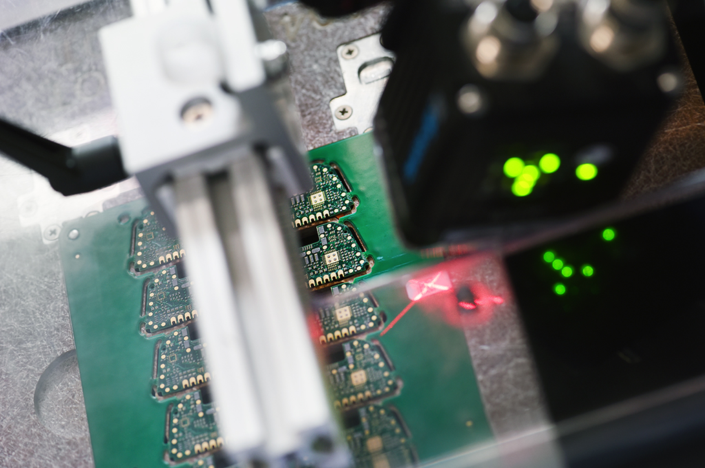
Solder paste printing
The unique printer kind is used for solder paste applications during the PCB assembly process. This type of printer is widely called a squeegee blade printer. It got its name from squeegees used to press the solder paste across the stencil surface and inside the PCB holes. They may be made either from metal or polyurethane, depending on the pressure ranges they need to generate. The printer's internal vision system aligns the stencil vertically over the boards. In addition, the printer uses three fiducials, commonly called global fiducial marks, for the stencil's highest precision positioning over the board. Namely, the global fiducial mark immediately determines and corrects any eventual PCB misalignment in both the X and Y axes before printing operation and during the printing as well. In that way, the possible displacement of either board or stencil under pressure generated by the squeegee is completely avoided.
Squeegee pressure is a parameter that must be controlled with special attention. Increased pressure may cause multiple issues such as greater paste shear that causes paste spreading over the PCB flat surface and causes so-called bridging and bleeding of solder paste. Since the paste is a highly viscous suspension, it requires significant force to flow. The squeegee pressure must be sufficient to generate the force that overcomes the high friction force between the highly viscous paste and the stencil. Once paste movement is initiated, the paste travels across the width of the printable area in a controlled roll, filling in all stencil apertures while simultaneously being swept from the top side of the stencil surface by squeegee blades. The standard operating pressure range of the squeegee is between 0.13kg and 0.27kg per linear centimeter of the printable area. The moving squeegee must induce inertia under whose influence the paste flows inside the PCB holes. Abrupt but controlled motions of squeegees induce inertia, which is why the speed is another parameter that must be monitored continuously. Since the squeegee's pressure and speed are directly proportional, the speed must be continuously below the upper constraint value, usually 75mm per second. The higher speeds induce the higher friction force between the blades and stencil, leading to blades' mechanical failure over time.
The third essential parameter of solder printing is the angle between the squeegees and the stencil. The regularly set angle is 60° for the following reason. It forms an optimal incline, so the paste moves downwards to the PCB holes by gravity. If the angle increases, it can cause scooping of the holder paste out of the stencil apertures and consequently an insufficient amount of solder paste. On the contrary, the blades leave a solder paste residue on the stencil after the squeegee has completed a print when the angle decreases.
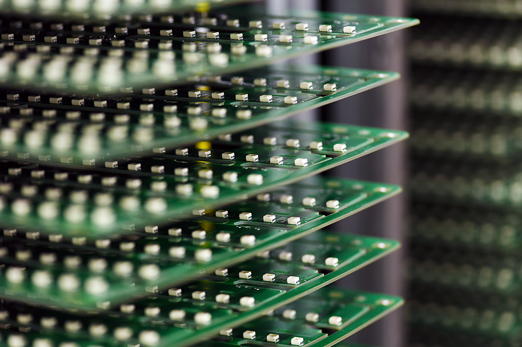
A regular printing operation lasts between 15 to 45 seconds per print circuit board. The printing is the longest step in PCB assembly, followed by the separation process in which the stencil is separated from the PCB. Postprint inspection is essential for quality assurance of deposited solder paste layers and their suitability for the following step-surface mounting of electrical components. The quality assurance is usually performed with unique 2D vision systems on the printer or separate 3D systems.
Stencil separation and cleaning
The PCB is separated from the stencil at the end of the printing process. During separation, the solder paste must remain in the PCB holes. The speed of stencil removal is crucial to ensure that the stencil doesn't withdraw any paste from apertures. The regular linear speed of stencil movement is around 3mm per second. The solder paste can't fully release from the apertures at higher speeds, causing undesired high edges around the deposits.
After few printing operations, the stencil cleaning ensures that there is no accumulation of the paste particles between the stencil and the PCB. The cleaning operation is comprised of two steps: Firstly, the stencil is swept using cleaning chemicals like isopropyl alcohol. In this step, the area underneath the stencil is cleaned. Then, additional vacuum cleaning occurs where the apertures are cleaned to avoid blocking paste flow to PCB holes.
Quality assurance of stencil and squeegee condition after a printing session
Before quality assurance of mechanical parts, the automated cleaning system removes the solder paste residues altogether, so the operator has a clear view of the entire material surface. Then, the operator proceeds with a visual inspection of stencils and squeegees to check if any mechanical defect arose on both blades and stencils. If the operator notices any damage on squeegees or stencils, he needs to replace a defective part to provide a reliable and efficient printing process.