The demand for professional electronic manufacturing services (EMS) rises from year to year due to the rapid increase of the electronic components market. The "Global Electronic Components Market 2020 Research Report" published a report stating that the global market for electronic components is predicted to grow at a compound annual growth rate (CAGR) of around 4.8% from 2020 to 2025. As a result, electronics applications are becoming abundant in many sectors such as medical, industrial automation and motion control, the automotive industry, and many more. Still, the functionality requirements are becoming more demanding, which is why the Semecs team follows the latest technology trends to deliver the highest quality products to our customers.
Electronics Manufacturing Applications
Semecs provides a whole range of electronic manufacturing services with a primary focus on the three industries.
Medical
The PCBs in medicine found their role in various applications such as medical imaging, monitoring devices, and implantable medical devices.
Monitoring Devices
Various medical monitoring devices utilize PCB technology to display information received from the sensors. Some devices that need PCBs for their application are bodily temperature monitors, blood pressure monitors, and blood glucose monitors.
Medical Imaging/Diagnostic Devices
Medical imaging devices are nowadays the essential equipment that we should be grateful for prevention and discovery of various diseases at an early stage. Magnetic resonance imaging, computerized axial tomography, and ultrasound equipment possess PCBs that decode complex signals to comprehensive information visualized later on.
Implantable medical devices
The PCB is an integral part of numerous implantable medical devices. Those types of PCBs are incredibly tiny in size in comparison with standard-sized ones. Boards are connected to small batteries that present the permanent source of electricity. Some of the implants that require the PCB to control their operations are pacemakers, implanted defibrillators, and cochlear implants. Each of those devices must operate specifically according to the doctor's diagnosis. Hence, the PCB manufacturing of implantable devices must be very flexible since each patient has specific needs.
Industrial
Industrial applications are endless, from process automation to motion control using robots. Industrial engineers strive to optimize manufacturing operations' productivity by increasing throughputs while minimizing costs, so it is essential to have PCBs that operate at the highest level. Namely, the great benefit of automation is cost reduction since large production throughputs are enabled in shorter periods with the minimum requirement for the labor force.
Automotive industry
The PCBs are an essential part of both autonomous and conventional vehicles. Due to rapid technological improvements, many clients from this industry have new requests for electronic manufacturing services (EMS) within a few months. The size requirements are pretty strict when it comes to PCB applications in the automotive industry. Space is often limited, so manufacturers must be very flexible during the manufacturing stage to fulfill all requirements. PCBs have various applications from running lights, transmission controls, and comfort control units. Additionally, PCBs manage engines, entertainment systems, digital displays, radar, GPS, power relays, timing systems, mirror controls, and many more.
Industrial design
The PCB design made by our clients represents a set of precise requirements. Therefore, we use it as a guideline through the PCB manufacturing process. To provide the best electronic manufacturing services, the manufacturers must efficiently convert received Gerber files into optimal 3-D design using CAD software like Fusion 360.
Clients provide open ASCII vector files containing information on each physical board layer of PCB design. The Gerber file must include circuit board objects for successful industrial design, like copper traces, vias, pads, solder masks, and silkscreen images. All mentioned parameters are written in the form of the flash or draw code and defined by a series of vector coordinates. Here at Semecs production facilities, we use this data to convert all details into the physical properties of the PCBs that will be realized during the manufacturing stage. In the provision of electronic manufacturing services (EMS), the optimal solutions are the ones that decrease the manufacturing costs and reduce required board space without sacrificing product quality.
Our ultimate goal is to deliver the optimal industrial design within set mechanical and power constraints. The industrial designer chooses the optimal materials for PCB assembly while the number of layers within each PCB and the copper traces presenting electrical pathways are predefined by the customer. The mechanical restrictions define the limits, such as the shape and size limits of the PCB, and we always consider them. Besides having in mind the mechanical restrictions, our team proceeds with industrial design taking care of power restrictions. Every single SMD component at the board has upper power limits it can withstand. Therefore, the appropriate component arrangement is crucial for the successful operation of PCB. A power design guideline must be structured to expose all components to signals, voltages, and amperages according to their specifications. Therefore, adequate voltage separation is essential to design print circuit boards according to power restrictions. For undisturbed current flow, it is best to use standard rails for each supply, avoid longer power loops in routing, and possess traces with wide diameters. On the other side, the board bending is avoided by separate power and ground planes. The everyday practice at Semecs facilities is placing a minor impedance path to prevent the risk of higher power circuit interference.
New product introduction and prototyping
Even when the clients provide PCB design and a complete list of specifications and requirements within the Gerber file, industrial-scale PCB manufacturing is far from reality. The PCB design from the Gerber file is a set of various data, and designers must proceed with the feasibility study and preliminary 3-D plans to ensure the compatibility of the primary set requirements and actual manufacturing that will take place. It is rarely the case that there is only one feasible manufacturing pathway, so various design options are discussed during the prototyping stage. The primary purpose of the prototype design process is to provide the experimental PCB sample that fulfills the primary set requirements. The prototyping is often a time-sensitive stage where clients want to ensure that the production of their product is a viable investment, and our engineering team with decades of experience ensures that the prototype sample is assembled and tested promptly. Once the functionality is achieved, our team discusses all further design aspects with the client. At this stage, the product development portion of the design process occurs while the ultimate goal is to optimize the prototype for industrial production that will be cost-effective. Therefore, the potential changes for manufacturability and product performance, and life cycle are discussed.
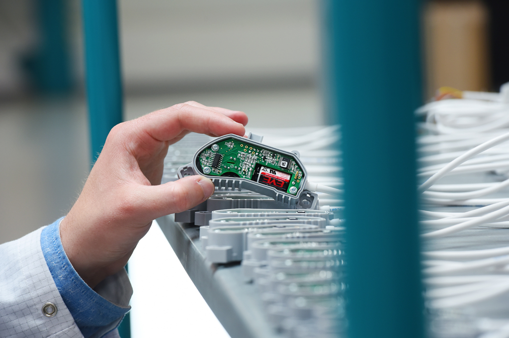
PCB manufacturing
PCB manufacturing is the heart of the electronic manufacturing services (EMS) since all previous steps are related to consultation and delivering functional PCB samples as prototypes. Before proceeding with PCB manufacturing, the Semecs team upgrades the prototype by adding all
previously defined technical and aesthetic features. The large volume production of the unique PCB boards requires the highest precision of every detail from the early beginning. First, the chosen board material should be cut to the required dimensions and then cured in the oven to ensure that it is ready for manufacturing. Next, the thin film containing the complete scheme of electrical pathways is applied onto the board substrate using a plotter. The film comprises two layers, inside and outside ones. The inside layers contain two ink colors where black ink represents electrical circuits while clear ink represents non-conductive areas. In contrast to the inner layers' design, the exterior layer design is reversed. During the manufacturing stage, special chemical compounds such as epoxies are used for removing excessive areas from the board in the following way. First, they cover the particular area on the board. Then they are exposed to the UV light that causes their hardening. Finally, the unhardened areas are etched off, meaning that only designed parts remain within the board construction. After film application, numerous processes occur sequentially to produce the highest quality PCBs, and they are described in-depth on the PCB manufacturing service page.
Once the structure of the printed circuit board is finalized, the board is ready for solder paste application. Namely, the solder paste should be applied onto parts where SMD components will be mounted later on. The squeegee blade printer is used for this application. The blades distribute the solder paste across the board surface, while the final aim is to fill the small cavities representing the areas for electronic component placement. The speed of stencil removal is the most critical parameter that ensures that the stencil doesn't withdraw any paste from apertures. The common linear speed of stencil movement is about 3mm per second. The solder paste can't fully release from the gaps at higher speeds, causing undesired high edges around the deposits. So, the paste must end up in cavities while the surface should remain intact because otherwise, the so-called bridging could occur, leaving the board unfunctional. The printing is the most demanding step in the PCB assembly, representing a bottleneck for many PCB manufacturing companies. Still, we at Semecs succeeded in reducing its duration to 15 seconds. The efficient solder paste application is essential for the firm and stable bonds formed during the surface mounting that will take place in the next stage of PCB manufacturing.
Once the printing process ends, the SMD components are mounted on the PCB surface using surface-mount technology. This technique is outstandingly efficient in terms of the component placement speed and strength of the formed bonds between the components and the board. The pick and place machine is responsible for component positioning at their designed places at PCB. This machine is programmed to recognize each SMD component by its code and follow the scheme from the Gerber file. Finally, the robotic arm takes electronic components and places them at the PCB's surface.
At this moment, the solder is still in the form of a paste, and it needs to harden to fix the component permanently to the PCB surface. The hardening process occurs in the curing oven, where boards move on the conveyor while hot air at high temperatures heat them.